
Field-Programmable CV Jacks
alchemy-lab · alchemy-sdk · hardware-design
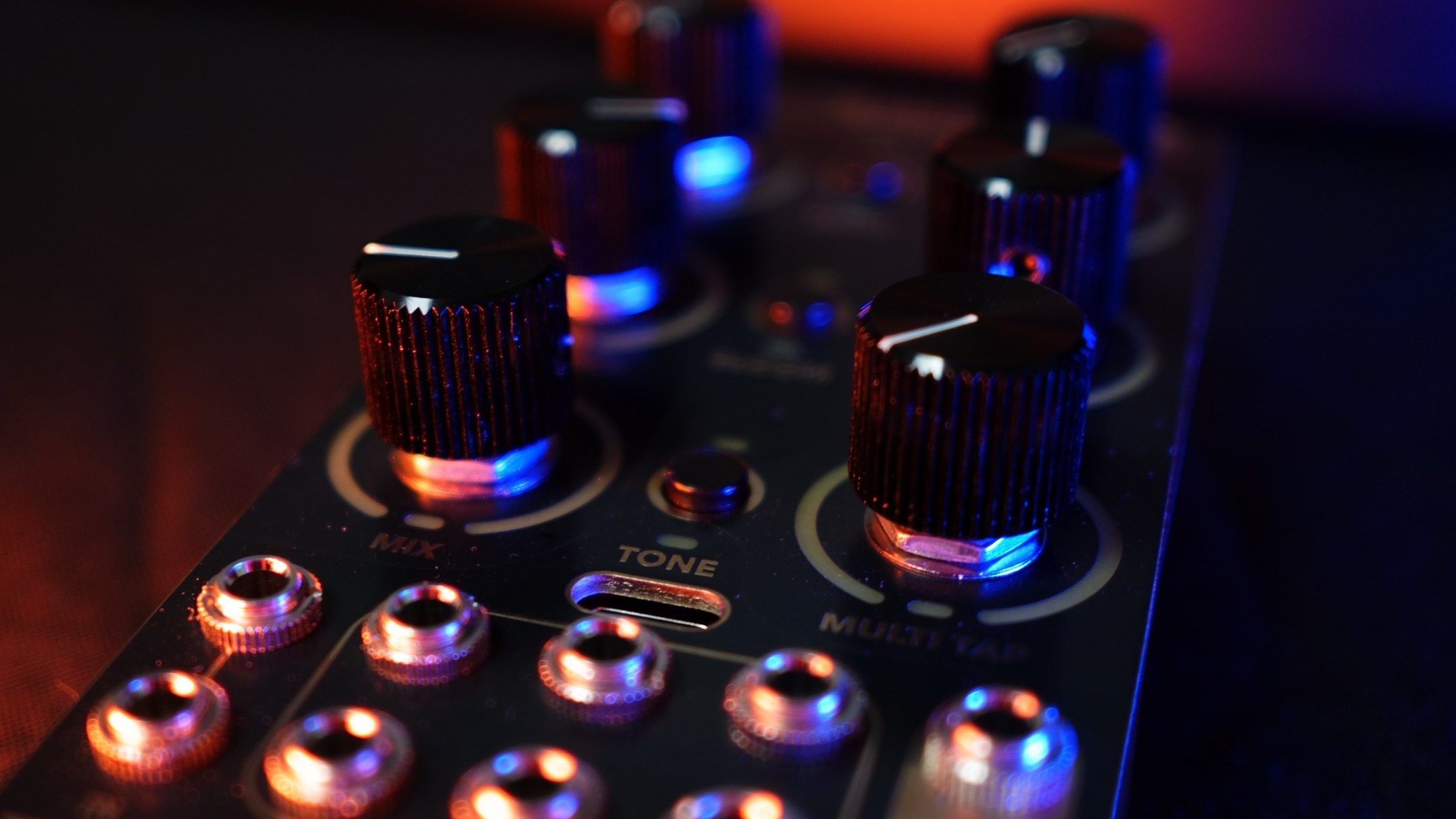
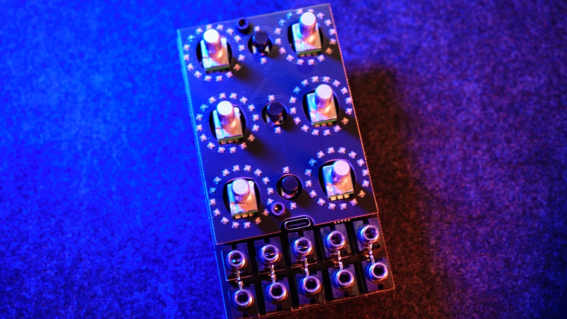
Field-programmable CV jacks! On the Alchemy Lab, six of the ten panel jacks (J3 through J8) switch between CV input and CV output at runtime: at boot, per preset, or live at any time. This post documents the mechanism, because I have not seen it explained anywhere else in Eurorack: the analog switch behind each jack, the op-amp stages on both sides, and the three DAC backends.
Beyond fixed panels
A digital module is one panel with many firmwares, and every firmware inherits the I/O layout of the PCB. But different firmwares want different layouts. A delay wants a clock input and modulation inputs; a function generator wants outputs; a sequencer wants both. Whatever the designer picks, some firmware ends up with dead jacks or contrived purposes for those jacks: inputs it cannot use, outputs it cannot offer.
The usual responses are to ship more hardware, an expander per use case, or to accept the waste. I wanted something cooler. I started with jumpers: duplicating the CV scaling circuit, putting the jack tip on the middle pin, and jumping to either network. But this kind of sucked. You had to pull out the module, I was always forgetting what state it was in, and users would have this obnoxious caveat of having to declare a jack jumper layout with every firmware. I found a much better solution.
What Switching Looks Like From Firmware
The Alchemy SDK exposes each jack as a CvJack with the same public methods regardless of what is wired underneath:
hw.j3.EnableCvOutput();   // close the switch: J3 is now a CV output
hw.j3.SetVolts(2.5f);     // +2.5 V at the panel
hw.j3.DisableCvOutput();  // open the switch: J3 is a CV input again
float v = hw.j6.Volts();  // calibrated input read, in volts
EnableCvOutput() routes a backing DAC onto the jack, DisableCvOutput() disconnects it, and both calls are legal at any time. The SDK ships an example, cv_playground.cpp, in which button B2 flips all six jacks at once between output mode, where each jack emits a free-running saw wave and its LED ring spins an orange pixel, and input mode, where each ring becomes a voltmeter for whatever is patched in.
How Does the Switching Circuit Work?
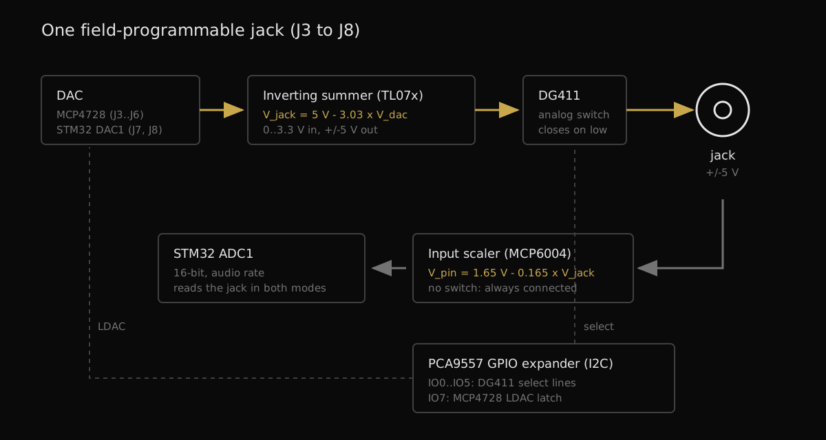
Each of J3 through J8 sits behind one channel of a DG411 analog switch. The switch either connects the jack to its DAC's output stage or leaves it disconnected. The input path has no switch in it at all: the ADC always sees the jack. Direction is therefore not a mux flipping between two paths; this would require many more switches. Output mode just means a DAC is currently driving the node the ADC is already watching. This works because the input path doesn't "leech" voltage from the DAC output, but if we were to attempt to read incoming CV with the DAC connected, the analog front end would bias the incoming CV signal on the DAC's side. This is just a simple property of source impedance and the direction of the resistor network. I leave calculation of this as an exercise for the reader.
You don't need to reboot or flash firmware to switch jack directions.
The SDK initializes the expander with every select line high, and the DG411 opens on a high control input, so every jack is an input until firmware explicitly says otherwise. A crashed module or a half-flashed firmware presents a panel of passive inputs, which can be nice in the event a CV input source you have patched in is poorly designed.
Making ±5 V From a 3.3 V DAC
The classic scaling circuit. The DACs on the board produce 0 to 3.3 V. Eurorack CV wants ±5 V. Between each DAC and its switch sits an inverting summer, a TL07x op amp running on the module's ±12 V rails, that maps one range onto the other:
V_jack = 5 V - 3.03 x V_dac
DAC code 0 therefore produces +5 V at the panel and code 4095 produces -5 V. SetVolts() inverts a per-jack linear fit, an offset and a gain the board measures for that specific jack during self-calibration, clamps to the 12-bit range, and writes the code. Near the ends of the range the output stage compresses against the DAC's supply rails and stops tracking the fit, but the SDK clamps to code 0 or 4095 anyway, because landing as close to ±5 V as the analog stage physically allows matters more than perfect linearity in the last hundred millivolts.
The input direction does the same in the other direction. An MCP6004 stage maps ±5 V at the jack into 0 to 3.3 V at the STM32's ADC pin (V_pin = 1.65 V - 0.165 x V_jack), so a high ADC code means a negative jack voltage. By the way, you use an MCP600x for input because it works with a narrow supply range on voltage (0 - 3v3), and you use TL07x because it's better in those 24v Eurorack spans.
This is the classic Mutable Instruments approach!
Three DAC Backends to save money
"The DAC" is really three different pieces of hardware depending on the jack. J3 to J6 share an MCP4728, a quad 12-bit DAC on the I2C bus. J7 and J8 use the STM32H7's two internal DAC channels, which are memory-mapped and settle in under a microsecond. And J9 and J10, the DC-coupled codec outputs, can be claimed as CV outputs too: EnableCvOutput() on those takes the channel away from the audio callback, and the SDK fills each audio block with the current SetVolts() target at 24-bit resolution.
| Jacks | Backend | Output resolution | Output latency | As input |
|---|---|---|---|---|
| J3 to J6 | MCP4728 over I2C | 12-bit | ~70 µs | 16-bit, audio rate |
| J7, J8 | STM32 DAC1 | 12-bit | <1 µs | 16-bit, audio rate |
| J9, J10 | Audio codec, DC-coupled | 24-bit | one audio block | output only |
The point of the table is what never appears in user code: none of these differences leak through the API. CvJack dispatches on its backend internally, and the public methods behave identically on every jack. Firmware picks jacks by what makes sense on the panel.
Latching Four Channels at Once
The MCP4728 introduces a coordination problem the other backends do not have: four jacks share one chip on one bus. When a firmware repatches several jacks in the same control frame, and a preset change is exactly that, naive per-channel writes would ripple the four outputs into place over separate transactions. Ultimately, not a huge deal, but we handle this with the LDAC line in a sort of batched writes scheme in the SetVolts() as a best practice.
What a Real Firmware Does With It
Echoa, the delay I launched the platform with, runs all six switchable jacks as inputs and shows what the routing layer above this hardware looks like. Each jack routes to one of 23 destinations: five gate-style specials (tap tempo and freeze, per delay line) and 18 continuous destinations, every pot on every page. Each jack carries its own bipolar attenuverter, and jacks pair with pots by panel geometry, a quarter-turn counterclockwise rotation that is its own inverse. The firmware side of this kind of routing is six lines of CvMatrix code, which the 117-lines walkthrough covers.
Echoa uses a fixed all-inputs assignment. The switching hardware means the next firmware need not agree. A sequencer on the same panel can claim four jacks as pitch and gate outputs. A firmware can reconfigure I/O per preset, so one preset's modulation input is another's envelope output. An instrument that ignores its inputs can hand them back as LFO outputs instead of letting them sit dead.
Engineering Notes
The DG411 closes on a logic low; its sibling the DG412 closes on high. Every write goes through kDg411OnLevel, so if a future board revision swaps the part, the port is a one-line change. But the DG41X parts are quite nice, I'm not sure what part could be an adequate substitute.
The two audio inputs earn their keep as trigger jacks. J1 and J2 are AC-coupled codec inputs, so they cannot read a static CV, but edges pass through the coupling capacitor cleanly. The SDK thresholds them at block rate and exposes RisingEdge(), a perfectly good clock or trigger input for firmware that does not process external audio, which frees switchable jacks for other work.
Everything described here is MIT-licensed and shipping. The routing tables, the constants, and the CvJack class live under hardware/alchemy-lab/v2/ in the Alchemy SDK repository; the developer page covers setting up a toolchain, or you can skip the toolchain and use the browser flasher. If you build a firmware that repatches its own panel, I would genuinely like to see it: join us on Discord.
FAQ
Can a jack be damaged by patching into it while it is an output?
No. Every Alchemy Lab jack tolerates up to ±12 V at the panel, the worst case a Eurorack system can patch into it, whether the jack is set as an input or an output at the time. The usual rack rules still apply: nothing beyond ±12 V, no mains, no speaker-level signals.
How fast can a jack change direction?
The direction change is one register write to the I2C GPIO expander, about 75 microseconds at 400 kHz, and the analog switch itself settles in well under a microsecond. A live repatch completes within a single control frame.
Do the jacks default to inputs or outputs?
They default to inputs. The GPIO expander boots with every switch open, so a jack becomes an output only when firmware explicitly claims it.