
WS2812 Without PWM: Driving 102 LEDs With TIM6 and DMA
alchemy-sdk · hardware-design · embedded-engineering · daisy
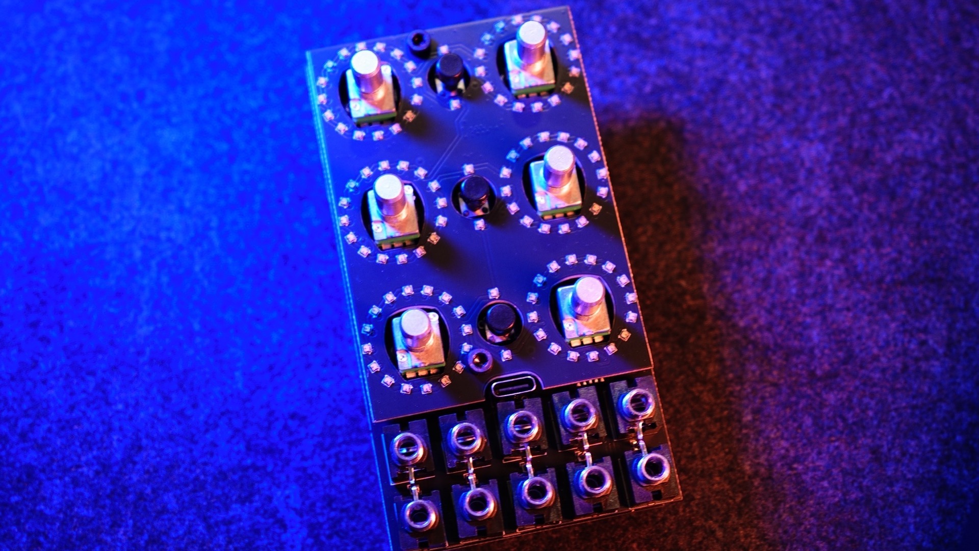
The Alchemy Lab has no screen. Or, it's almost all screen, depending on how you look at it. Its entire display is 102 WS2812-family RGB LEDs: sixteen around each of the six pots, plus two per button. Every animation an instrument renders passes through one driver, and that driver has a story of how it came to be. When we laid out the V2 board, the LED data line landed on pin PD11, and PD11 has no timer PWM channel on the STM32H7. The standard way to drive WS2812s from an STM32 was physically unavailable on the pin we had routed. Unfortunately, various factors forced this pin to be used, so we had to work with that sadly poorly equipped pin.
This post explains what we did instead: a basic timer that owns no pins, a DMA stream pointed at a GPIO register, and a 32 KB window of RAM that the CPU cache is forbidden to touch. The whole driver is 325 lines, open source, and worth reading if you have ever needed a precisely timed digital waveform on an arbitrary pin: ws2812.cpp.
Crediting prior art here: the family of tricks this driver belongs to is well established. Paul Stoffregen's OctoWS2811 has been generating WS2811 waveforms with DMA writes to GPIO since the Teensy 3.0 era, and Martin Hubáček's STM32 WS2812B DMA library brought the same idea to STM32. Both were built to drive many strips in parallel, and both spend three DMA channels keyed to different timer edges: one sets every pin high, one writes the data, one pulls every pin low. What is actually new here is a small spin: a single DMA stream on a single pin, an encoding that spends one precomputed BSRR word per sub-cell and uses the register's no-op as its third symbol, and the Cortex-M7 cache discipline that the classic F1, F3, and F4 targets never had to think about because they have no data cache. You might also find this pattern useful!
Why WS2812s Are Picky
A WS2812 has one data input and no clock. Every bit is encoded in the width of a high pulse inside a fixed 1.25 microsecond window: a short pulse is a zero, a long pulse is a one, and a line held low for longer than the latch time tells the chain to display what it received. The timing tolerances are hundreds of nanoseconds wide. At 480 MHz that sounds generous, but a CPU that is also servicing audio DMA, USB, and a control loop cannot promise nanosecond-stable loops, which is why bit-banging WS2812s is a no.
The textbook fix is hardware: run a timer in PWM mode at 800 kHz, and have DMA rewrite the compare register before every period, so pulse widths come out of a precomputed buffer with no CPU involvement. Our V1 development board did exactly that, with TIM3 channel 4 feeding the LED pin. The catch is that this recipe requires the pin to be wired to a timer output channel. PD11 is not. V1's code could not port, and rerouting the board for the timer's sake was the wrong trade.
Also - for audio applications, I, in the end, wish I had used a two wire WS-style LED. But I'm not sure any exist in a 1010 package, and packing 16 around a pot is difficult even with a 2020 package. But I digress...
Pinless timers
The replacement rests on two observations.
First, a timer does not need pins. Obviously. I point it out because we're so used to linking a timer to a pin as embedded engineers. The driver runs TIM6 at 2.4 MHz, three times the WS2812 bit rate, so each 1.25 microsecond bit window is divided into three sub-cells of 417 nanoseconds. The timer's only job is to fire an update event at every sub-cell boundary.
Second, the GPIO port's BSRR register was designed for exactly this kind of abuse. Writing a word to BSRR sets the pins named in its low half, resets the pins named in its high half, and, critically, does nothing for pins named in neither. Writing zero is a perfect no-op. That gives us a language of three words for one pin: set, reset, and hold.
Wire the two together and the driver falls out: DMA1 Stream 7 is triggered by every TIM6 update event and copies the next precomputed word from a buffer into GPIOD's BSRR. The pin is configured as plain push-pull output with no alternate function. In this way, they are disconnected, linked only by the implicit contract of the words.
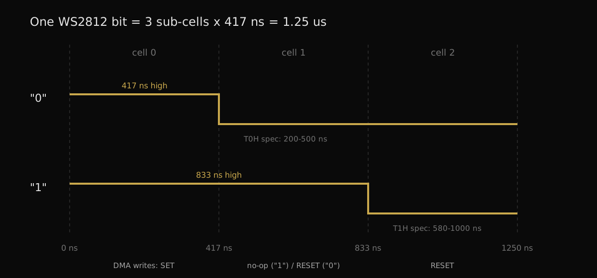
Encoding a bit takes three words. Cell 0 is always SET. Cell 1 is the bit. A RESET word ends the pulse at 417 nanoseconds and encodes a zero while a no-op word holds the line high through 833 nanoseconds and encodes a one. Cell 2 is always RESET. After the last pixel, the driver appends 720 no-op cells, roughly 300 microseconds, then we latch.
Three 32-bit words per bit, 24 bits per LED, 102 LEDs, plus the latch tail: 8,064 words, or 32,256 bytes. The buffer lives in a dedicated 32,768 byte region. The maximum chain length in ws2812.h is kWs2812MaxLeds = 102 because the panel has 102 LEDs and the window has 32 KB.
Kind of excessive, but I am working on future boards with more LEDs and I don't want to footgun myself in the future. Because let's be honest, I'm going to have to relearn this whole system from scratch, in part by re-reading this blog. Code written two weeks ago was written by someone else.
Caching makes party mode, in a bad way
This part sucked. The Cortex-M7 has a data cache, and DMA does not read through it. Write your buffer normally and some of those words sit in cache lines that have not reached RAM when the DMA fires; the LEDs then display a mix of new and stale data, differently every frame. Cache incoherence does not look like a crash. It looks like haunted glitter. I have weird videos to prove it. This was extremely difficult to debug and ID, because the LEDs all "worked" - except they'd randomly go into full gamer PC case party mode at random moments.
The driver's answer is to make the buffer non-cacheable at the architecture level. The linker places the cell buffer in its own NOLOAD section at address 0x30008000, and at init the driver programs MPU region 3 to mark those 32 KB non-cacheable, using the same attribute set libDaisy applies to its own DMA window at 0x30000000 (libDaisy owns MPU regions 0 through 2; region 3 was free). Order matters and the code is explicit about it: the region is configured before the buffer is ever touched, and any cache lines that might already alias the range from earlier boot-time accesses are cleaned and invalidated so they can never be evicted over fresh data. Because configuring the MPU means briefly disabling it, the whole sequence runs during board init, before audio DMA exists to race against.
You can't skip this part. Trust me.
What It Costs
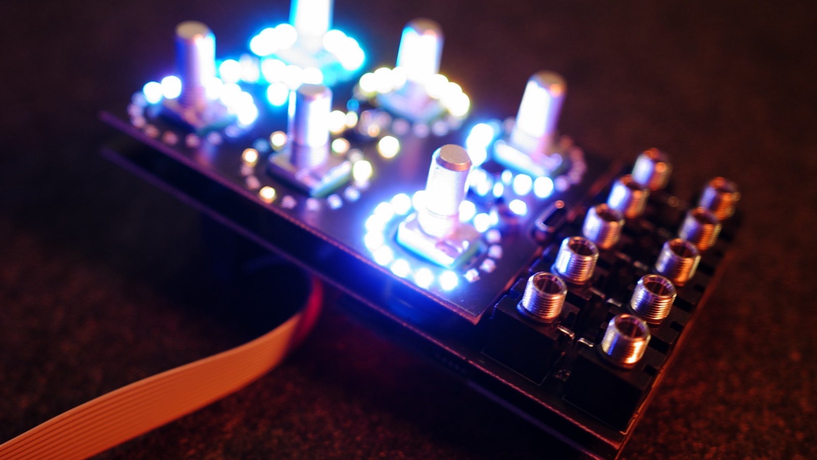
One timer, one DMA stream, one interrupt, and 32 KB of RAM. The CPU's only work is re-encoding the pixel buffer when a frame changes (you can control the frame rate in the SDK); the wire timing itself is handled by DMA + timer for zero cycles. On top of this driver sits the SDK's ring animation system, which repaints the panel at roughly sixty frames per second at default.
The pattern is not WS2812-specific. Timer update events plus DMA-to-BSRR will produce any precisely timed digital waveform on any GPIO, at the cost of one word of buffer per timing cell. If you are laying out a board, you can skip all this if you route your LED data to a timer pin and use the textbook recipe. If the layout already happened, or you end up constrained like me, this is the escape hatch. It's MIT, you can copy it.
In fact, the driver, the board support package it belongs to, and the whole Alchemy SDK are MIT-licensed. If you build something with it come tell us on Discord.